Semiconductor Capital Equipment Market by Type (Assembly equipment, Automated test equipment, and Wafer level manufacturing equipment), by Application (Foundries, Memory Manufacturers, and Integrated Device Manufacturer), by Industry (Consumer electronics, Information and technology, Telecommunication, and Others) - Global Opportunity Analysis and Industry Forecast, 2020 – 2030


 Speak to Our Analyst
The Global Semiconductor Capital Equipment Market size is estimated to be USD 18.03 billion in 2019 and is predicted to reach USD 35.31 billion by 2030 with a CAGR of 6.3% from 2020-2030. Semiconductor Capital Equipment is the industry involved in the manufacturing of component and devices used in the manufacturing of electronic appliances. The market is segmented to front end and back end, Front end is completely involved in the manufacturing process of such components and back end is involved in the testing, packing and supplying of these components to assembling site.

Market Dynamics and Trends
Over the period of time there has been increase in the demand of electronic appliances due to increase in disposable income and changing lifestyle with high standards of living. Moreover, increasing complex nature of advanced components and increased use of integrated circuits are expected to fuel the growth of semiconductor capital equipment market over the forecast period.
The factors such as increase in consumer electronics, coupled with rapidly evolving technology and increased demand of semiconductor memory devices for data storage are also expected to anticipate the growth of the market. However, lack of skilled labor and engineer are expected to hamper the growth of semiconductor capital equipment market. On the other hand, ongoing research and development, technological advancement and increased investment in electronics industry are expected to create lucrative opportunities in the market in near future.
Market Segmentations and Scope of the Study:
The global semiconductor capital equipment market share is analyzed on the basis of type, application, industry and geography. On the basis of type, the market is segmented into assembly equipment, automated test equipment, and wafer level manufacturing equipment. On the basis of application, the market is divided into foundries, memory manufacturers, and integrated device manufacturer. On the basis of Industry, the market is divided into consumer electronics, information and technology, telecommunication, and others. Geographic breakdown and analysis of each of the aforesaid segments includes regions comprising North America, Europe, Asia-Pacific, and RoW.
Geographical Analysis
North America represents the developed market due to the presence of developed economies and accounts for the largest market share. The other driving factors include presence of advanced technology, increased use of integrated circuits and others are expected to propel the growth of semiconductor capital equipment market.
Asia Pacific represents the developing economies with gradual increase in market share and rapid growth rate owing to the increased demand of consumer electronics, increased use of fabs, with increase in complex chip technology are expected to contribute the growth of semiconductor capital equipment market.
Competitive Landscape
The semiconductor market is fragmented and highly competitive in nature due to the presence of various market players contribute the market growth. Some of the major market players include Applied Materials, KLA-Tencor, Tokyo Electron, Advantest, Kulicke Soffa, Planar, Screen Semiconductor Solutions, Lam Research, ASML, Hitachi High-Technologies, ASM International, Rudolph Technologies, and Nikon among others.
The several recent developments taken place in the market in the recent past. For instance, In April 2019, Nikon Corporation has announced the release of the optical processing ma-chine “Lasermeister 100A.” This optical processing machine is a Nikon's proprietary metal processing machine that performs various metal processing with ease and with high precision using laser. Its capabil-ity encompasses additive manufacturing as a 3D printer, laser marking & welding and even polishing.

KEY PLAYERS:
- Applied Materials
- KLA-Tencor
- Tokyo Electron
- Advantest
- Kulicke Soffa
- Planar, Screen Semiconductor Solutions
- Lam Research
- ASML
- Hitachi High-Technologies
- ASM International
- Rudolph Technologies
- Nikon
Download Free Sample
Frequently Asked Questions


Related Report


Related Blogs
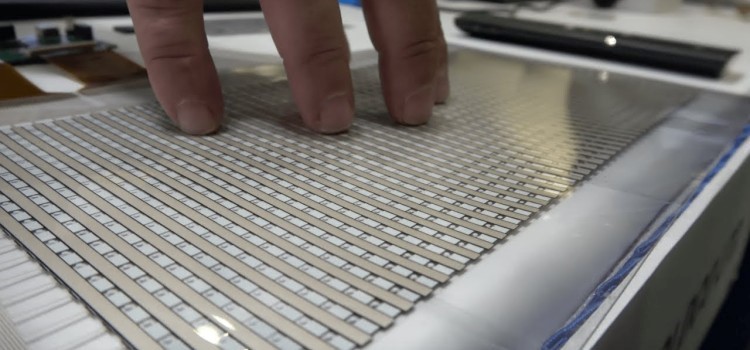
AI-Powered Tactile Sensors Revolutionizing Industry with Touch
Introduction In the landscape of industrial technology, the integration of arti...

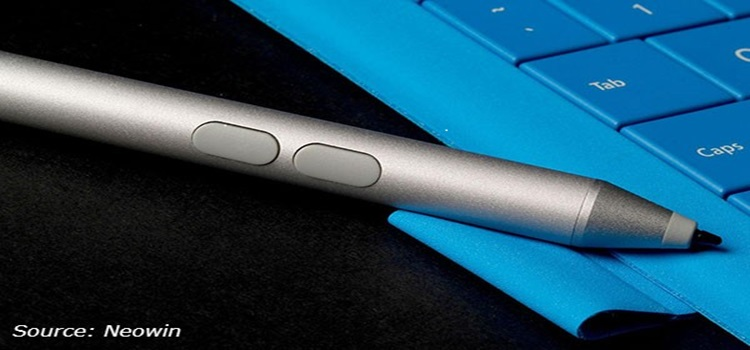
How Technological Advancements in Digital Pen is Reshaping the Market
Introduction As the digital pen market continues to evolve,...
Smart Dust: The Future of Sensor Technology
Introduction Smart Dust is a collection of several microelectromechanical systems (MEMS) such as sensors and other devices that c...